
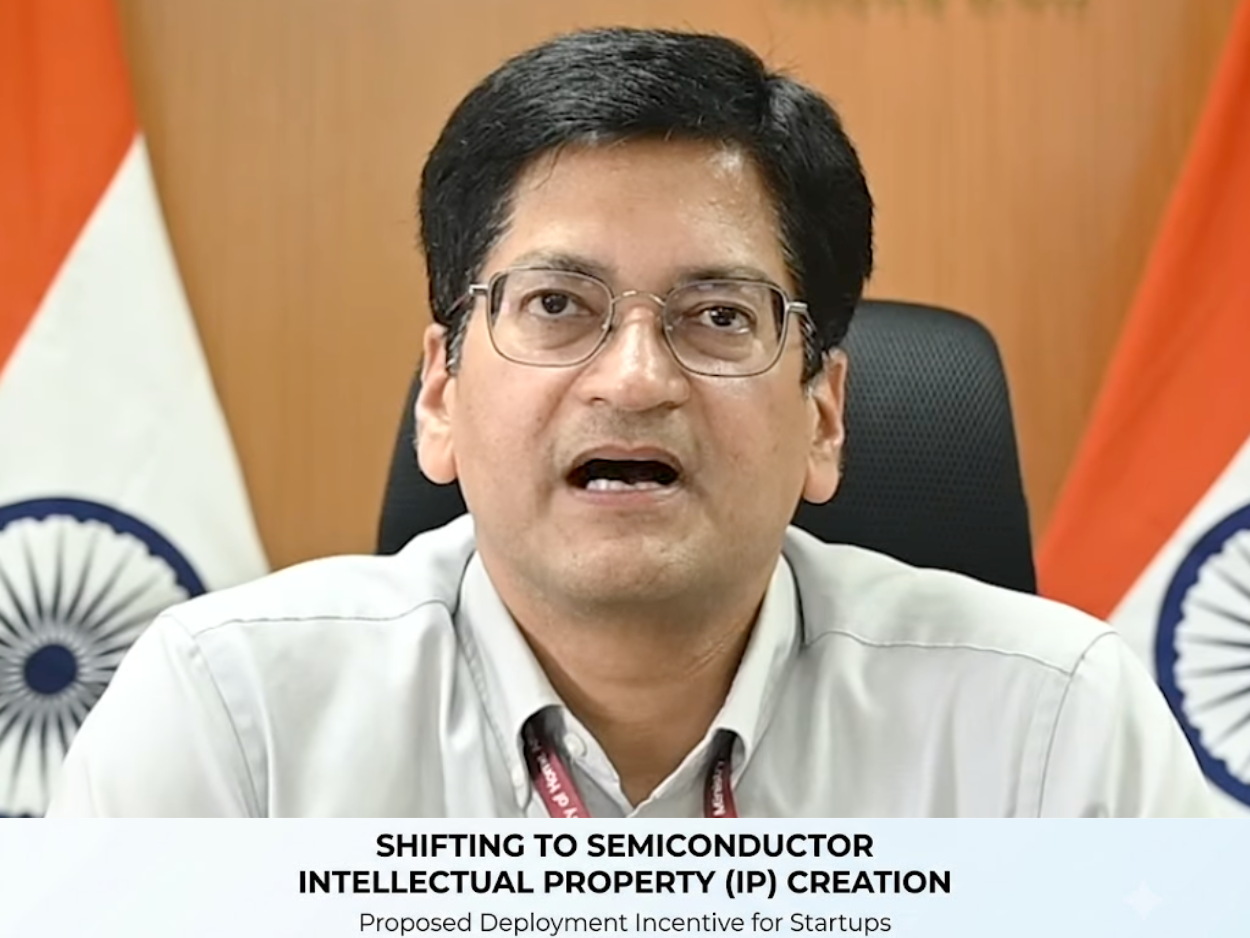
Amitesh Kumar Sinha Additional Secretary & CEO India Semiconductor Mission (ISM)
For the past few years, India’s semiconductor story has largely been told through steel and concrete new fabrication plants, OSAT facilities, assembly and packaging investments, and ground breaking ceremonies with foundation stones and ribbon cuttings. It’s been an uncomplicated story to tell, because it’s visible. You can point to a site, a construction timeline, or a job number.
A quieter shift is now underway, and it’s harder to photograph but arguably more consequential.
The Government of India is preparing to introduce a 9% deployment incentive for semiconductor startups under the next phase of the India Semiconductor Mission. According to ISM CEO Amitesh Sinha, the scheme is designed to offset the steep cost of prototype chip fabrication, the expensive, often make-or-break stage where a design either becomes a working chip or stays a very expensive idea on a hard drive.
It’s easy to read the announcement as one more line item in a long list of government schemes. It probably deserves more attention than that.
The Part of the Chip Story India Hasn’t Really Told Yet
Here’s a distinction that gets lost in a lot of the coverage around India’s semiconductor push: manufacturing a chip and designing a chip are almost entirely different businesses, done by almost entirely different people, at almost entirely different points in the value chain.
Once a chip arrives at a fabrication plant, its destiny is already mostly determined. How efficiently it performs, how much power it draws, what applications it can realistically serve – all of that gets decided months or years earlier, on a screen, by engineers writing and simulating circuit logic long before any silicon gets touched. That’s chip design. And it’s also where most of the semiconductor industry’s actual intellectual property – the patents, the proprietary architectures, and the stuff that generates licensing revenue for decades – gets created.
India has, until now, built an impressive amount of manufacturing capability without building much of this. That’s not a criticism; manufacturing had to come first, in some sense, because you need somewhere for a chip to actually get made. But an economy that only fabricates chips designed elsewhere is, in a very real sense, renting its position in the value chain rather than owning it.
Why Prototyping Costs Are the Real Barrier
If you talk to anyone who’s actually tried to start a chip design company in India or anywhere else, the conversation eventually lands on the same problem: getting from a design on paper to a working prototype chip is brutally expensive. A single fabrication run for a prototype can run into the hundreds of thousands of dollars, sometimes more, depending on the process node. For an early-stage startup, that’s often not a hurdle; it’s a wall.
This is precisely the gap the proposed incentive is aimed at. By offsetting a meaningful chunk of that prototyping cost, the scheme could let more design teams actually test their ideas in silicon rather than stopping at simulation. That matters more than it might sound, because a chip design that never gets fabricated and tested is, commercially, worth almost nothing. The value only really crystallises once a design has been proven to work, and that’s the exact stage this incentive is targeting.
What This Could Set in Motion
A stronger domestic chip design ecosystem doesn’t just produce more chips. It tends to pull an entire secondary industry into existence around it, one that’s arguably more durable than manufacturing capacity alone, because design talent, once built, tends to compound rather than depreciate.
Consider what actually needs to exist for chip design to thrive at scale: Electronic Design Automation (EDA) tools and the companies that build and support them. Verification engineers who can catch flaws before they become expensive silicon mistakes. Embedded software teams who write the code that actually runs on these chips. Packaging specialists who figure out how to physically house increasingly complex designs. Testing infrastructure sophisticated enough to validate performance claims. And, underlying all of it, a pipeline of VLSI engineers trained specifically for this kind of work — a skill set that’s genuinely scarce even in countries with mature semiconductor industries.
None of this appears automatically just because manufacturing capacity exists. It has to be built deliberately, and it tends to follow wherever design activity is actually happening, which is exactly why this incentive matters more than its headline percentage suggests.
What the Established Players Actually Did Differently
It’s worth looking honestly at how the countries usually held up as semiconductor success stories actually got there, because the popular version of the story tends to skip a step.
Taiwan is often cited purely for TSMC’s manufacturing dominance, but Taiwan also built a genuinely strong IC design ecosystem alongside it. Companies like MediaTek didn’t happen by accident; they happened because Taiwan invested deliberately in design capability, not just fabrication capacity. South Korea’s semiconductor strength rests on Samsung and SK Hynix, but a lot of the country’s competitiveness comes from tight integration between design, memory architecture and manufacturing, developed in parallel rather than sequentially. The United States, despite offshoring most of its actual fabrication decades ago, has retained an enormous share of global semiconductor value specifically because it kept design, IP and architecture companies like Qualcomm, Nvidia, and AMD design chips they don’t manufacture a single unit of themselves, and that’s precisely where most of their profit margin lives.
The pattern, once you look for it, is fairly consistent: manufacturing capacity is necessary, but it’s rarely where the largest, most durable economic value actually settles. Design and IP tend to be stickier, higher-margin, and far more resistant to being undercut by the next country offering cheaper factory-floor labour or land.
An Honest Note on Why This Is Hard
It would be a little dishonest to frame this purely as good news without acknowledging how difficult building a real design ecosystem actually is. Chip design talent takes years to develop properly; it’s not a skill that transfers cleanly from adjacent fields the way some manufacturing roles can. India already produces a significant share of the world’s VLSI and semiconductor design engineers, but a large proportion of that talent has historically ended up working for the design centres of global chip companies rather than Indian-owned startups building their own IP. That’s a talent retention and ownership problem as much as a funding one, and a prototyping incentive, however well designed, only addresses part of it.
There’s also the matter of time. Manufacturing announcements produce visible progress within a couple of years, a facility gets built, and production lines start running. A design ecosystem, and the IP portfolio that comes with it, tends to take considerably longer to show results, and the payoff is less photogenic along the way. That’s a real political and communications challenge for a policy aimed at long-term value creation in a news cycle that rewards short-term milestones.
The Ripple Effect
If this incentive works as intended, its effects are likely to show up well beyond the startups that receive it directly.
EDA tool providers and licensors would see rising demand as more Indian design teams move from concept to actual silicon, since virtually no serious chip design happens today without sophisticated simulation and verification software.
Verification and testing service firms stand to benefit meaningfully; every additional prototype run means additional demand for the specialised engineers and infrastructure needed to validate a chip actually does what it was designed to do before it goes anywhere near mass production.
Embedded software and firmware developers would find growing local demand, since a chip is rarely useful on its own; it needs software written specifically to run on it, and today much of that work for India-relevant applications happens overseas.
Packaging and OSAT facilities, including the kind of investments India has already been attracting, like ASIP’s Visakhapatnam facility, gain a more diverse, higher-value pipeline of domestically designed chips to package, rather than depending purely on contract work for foreign-designed products.
Automotive electronics and telecom equipment manufacturers are natural early customers for India-designed chips, given how much of India’s electronics demand already sits in these two sectors and how much value gets left on the table when the underlying silicon in Indian-made devices is designed elsewhere.
AI hardware and specialised computing startups could find this incentive particularly meaningful, since custom silicon is increasingly a competitive differentiator in AI applications, and prototyping costs have been one of the sharpest barriers keeping smaller Indian AI hardware teams from competing with better-funded global players.
Engineering education and training institutions would likely see downstream demand shift as well, with more pressure and more funding incentives to produce VLSI and chip design talent specifically equipped to build products, not just support foreign design centres.
The Bigger Picture
Factories are, without question, essential to a real semiconductor industry; nothing gets made without them, and India’s manufacturing push has been genuinely significant. But an economy that only manufactures chips designed somewhere else has capped, from the outset, how much value it can actually capture from the industry it’s building.
This proposed 9% incentive is a relatively small policy lever pointed at a fairly large strategic question: does India want to be a place where chips get made or a place where chips get invented? Those aren’t mutually exclusive, but they’re not the same ambition either, and the second one is considerably harder to build and considerably more valuable once it exists.
The manufacturing story will keep making headlines, and it should. But the more interesting question over the next several years might be a quieter one: how many chips shipping out of India, five or ten years from now, will actually carry Indian intellectual property inside them.